 Navigation
 Home
Home
 About Me
 Projects
 Blog
Blog
 Actions
 Go Back
 Top of Page

 Reverse-Engineering Jane Street's ASIC
 Posted: 2026-08-31 |
 Author: Siddharth |
 Category: Reverse Engineering
Reverse-Engineering Jane Street's ASIC
The ASIC
Jane Street put out a reverse-engineering challenge on their website. I had only known them for algorithmic programming challenges, so a reverse-engineering challenge was not something I expected lol. They also gave a warmup challenge for the people who had never done hardware reversing so try that out before you spoil yourself and read this blog . All the files are in this repository. Most reverse-engineering, crackme, and devirtualisation problems begin with a program you can run or load into IDA, but this challenge taught me reversing is more than that .
Jane Street's 2026 ASIC
puzzle has a binary, or should I say the program, was puzzle.gds:
the final physical layout of a small chip. The blog provided more information on what we are gonna be doing :
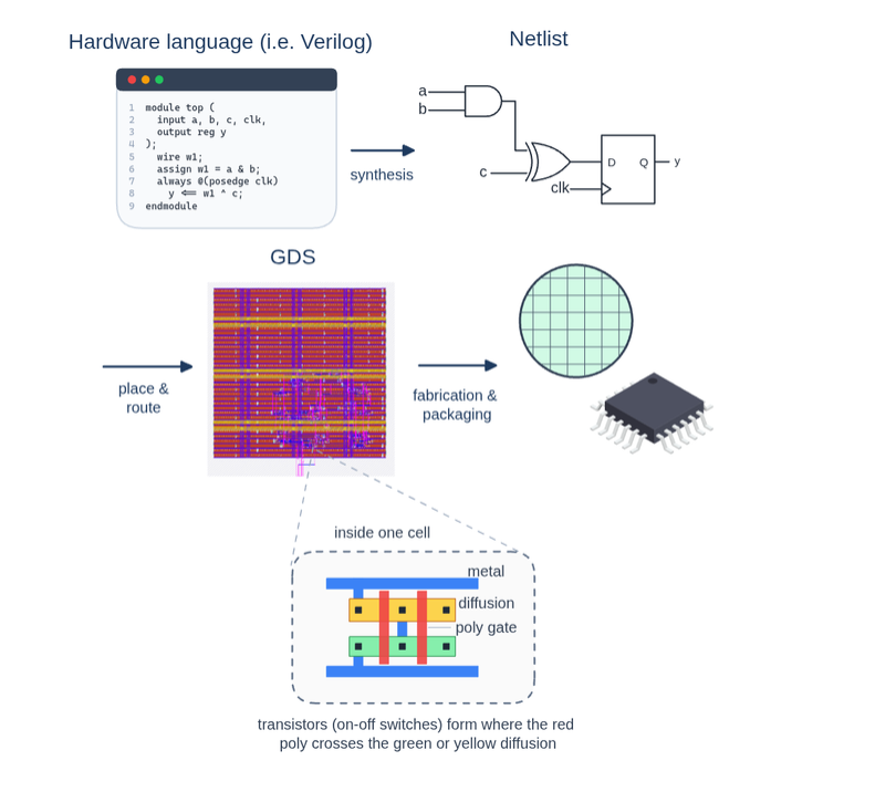
As with any reverse-engineering challenge, but here in the context of a chip, the question was: what would this circuit accept as a correct solution?
You can see the two problems here: a constraint problem and a reversing problem, which was much more fun to do, and hard. Before I could write a disassembler using something like Triton, or a symbolic solver using Miasm (is that even possible, because how does one emulate a clock without using things like LLVM-circt ?), to solve for an input, I needed to recover the wires hidden in the layout, attach those wires to the right gates, give every gate the right behavior, and model how the circuit changed on each clock edge. The biggest problem was that a single mistake anywhere could derail me and every step that followed.
Now that we know what to reverse, we can make a path similar to any VM crackme: find the VM dispatcher, find handlers, keep track of registers, write a disassembler, and solve for the path or basic block we need. Here, it could be something like:
polygons -> nets -> gates -> time -> constraints
If you don't have an electronics background, please read these before continuing:
- https://getwelsim.medium.com/gdsii-the-data-format-for-chip-and-integrated-circuit-design-012352970a54
- https://www.quora.com/What-is-a-GDSII-file-in-VLSI-and-what-information-does-it-contain-Can-anyone-provide-a-sample-GDSII-file-with-explanation
The GDS had enough supplied enough structural information to recover placements, pins, and candidate connectivity. Pinned SKY130 functional models supplied cell behavior, and the VCD supplied protocol evidence. This sounds like its gonna make our life easier but nope .
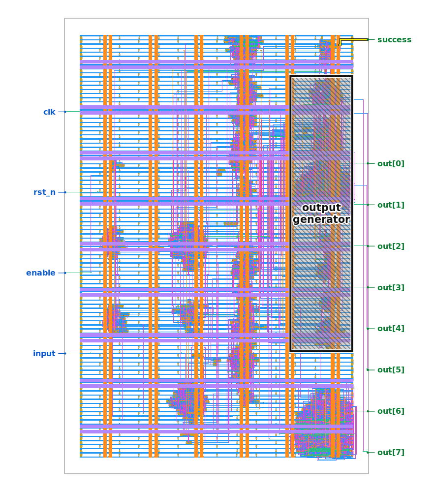
Figure 1. Full-chip layout with the output block marked.
A Program With No Source Code
A chip normally (should be right ? )starts as code , then a synthesis tool turns that code into a netlist(you will hear lot about this coming soon to read ), a list of logic cells and the wires between them,then a Place-and-route tools then put each cell at a physical location and draw those wires as metal. GDS records the result as something like polygons arranged in layers and grouped into reusable cells for the chip architecture
If you followd it till now , the puzzle gives us that last representation , if you still havent caught up think of this example ,consider a single inverter for that in a netlist it can be written as one cell with an input pin, an output pin, and two named nets so in GDS it will appear as an instance of a standard-cell layout placed at some coordinates and also small polygons will mark its pins. More polygons form wires on several metal layers. A via joins two layers where the design needs a vertical connection; the small opening used to form that connection is called a cut.
But the catch is that none of those polygons says, in anything that "this wire will carry or should carry the previous input bit" or "this gate checks the final result." The layout had retained some useful SKY130 standard-cell names and pin data inside the cell definitions, but the logical net names, behavioral source, and puzzle rules were gone just like your compiler kabboms it on -03 -strip.(could knoy think of this example , maybe someone can tell me a better example to connect with my non hardware reverse engineering audience )
So we have to treat the layout as a program with no source code.Like i said before in reference to devirtualisation ,the metal first had to become logical wires. Each standard-cell name should then become a Boolean function or a state update and the it hopefully solves ??
Coming back to designing our primitives for this challenge we have to solve which can be summed up as
- Which physical shapes are electrically connected?
- What Boolean or sequential behavior does each cell implement?
- What sequence of inputs takes the circuit to its accepting state?
Connectivity comes first as like this is obvious because a perfect model of an AND gate is useless if one of its pins has been attached to the wrong wire which would be very sad and cursed to debug
From Polygons to Nets
Recovering Cells and Pins
One thing if you read the blogs before (>u< read it !!) is that in GDS it is a one standard-cell layout that can be placed many times without copying all its polygons. Each placement will carry a cell name, a position, and possibly a reflection or rotation. A pin drawn at the left edge of a cell definition may therefore appear on the right edge of one placed instance and the left edge of another.(important !!)
We can use gdstk to read the file and apply each placement transform to the
polygons I needed. The puzzle has a flat hierarchy and on its top cell
contains 9,875 direct placements, and none of their cell definitions contains
another reference. A single pass over those placements was enough for this time , though it
would not be enough for if this had an arbitrary nested GDS
Ok So inside a SKY130 cell, datatype-16 polygons
on layers 67 and 68 marked pins. Texttype-5 labels supplied names such as A,
B, or Q so we can begin by matching each label to its local pin polygon, then transformed
that polygon into the coordinate system of the full chip. Datatype-20 polygons
on the same two layers will tell us the short pieces of routing drawn inside the
cell. Other rules (which iwill explain in a bit as you read) handles the metal above the cells and the cuts between
layers.
At this stage I kept geometry from every sky130* placement because even a
physical-only cell can touch a conductor. The logical build step i thought of planning it later. It
removed taps, decoupling cells, diodes, power pins, explicit via cells, and
other physical helpers. What remained was a flat netlist of 728 functional
cells. Ninety-two were flip-flops: 84 with reset, four with set, and four with
no async control.
Since every gate we had now could be names because of pins at coordinates the next plan was to decide which pin should belong to which wire (def not wanna mess this up )
Building Electrical Components RIP
Now imagine trying to following one signal out of a gate. It will begin at a pin polygon, crosses a short strip of metal inside the cell, joins a routed wire above the cell, and may climb through several metal layers before reaching another pin.But GDS stores those pieces separately. Now our extractor has to decide like do they form or even make sense that all of it aligns to one electrical component .
After transforming every selected polygon into top-level coordinates, I
converted it to a Shapely geometry https://github.com/shapely/shapely. Now after comparing all 63,463 shapes with every
other shape would have been wasteful and not the right approach obv lol , so an STRtree first found nearby
bounding boxes then we try to make exact geometric intersections which then to be decided whether each pair
should connect or nope
If you followed up until now , we can infer this as a reversing axiom/rule : two conductor shapes on the same layer joined when they overlapped with positive area. Mere contact at a point or edge did not normally count but the one exception we'll need to keep in mind is for pieces of internal routing drawn by the same placed cell(meaning - where some local routing pieces intentionally connect along an edge). Those pieces could join along an edge of positive length.
More thoughts - if we wanna move between layers , we need a different rule. An explicit VIA_* placement
contains conductor polygons for its landing layers, so the extractor should join
the polygons belonging to that via as one group. Standard cells also contain
implicit contacts. Their datatype-44 polygons are cuts, not metal. A cut on
layer L joined the conductor overlapping it on layer L to the conductor
overlapping it on layer L+1. (if you feel this is hard to understand , try out the warm up challenge which is in the same repo )
After this lets put each accepted join as a union operation in a disjoint-set, or union-find, structure.And at the end, every shape with the same root belonged to the same physical component. This helpes me to reduce the selected geometry to 3,986 components. However most actually did never touched a functional pin. After pin attachment and physical-cell filtering, the logical netlist used 739 distinct component IDs.
Also uhm these are not verilog singal names or sm but rather new labels for us to understand the layout connectivity.
The Netlists That Looked Right but Were Wrong smh
I did mess up a lot in the start tho , the final rules sound tidy now after a week of experimentation and crossing things off the list . My first extractors logic collected pins and top-level routing but ignored the cell-internal cuts. Another idea was to experiment with and treat every same-layer edge contact as a connection. That joined 1,365 components through touch-only paths, far too broad of a rule eventho i didnt know circuit design these are just too much to reverse . I replaced it with the limited same-instance exception described above.
The most stupid failure came in a later extractor. I made a broad condition selected datatype 20 or 44 on layers 67 and 68 before the code checked for cuts. This means that the low-layer datatype-44 shapes became ordinary conductors. The error was small in code but kinda devestating in meaning if you think about it : a cut connects the layers on either side of it but does not extend either layer sideways.
But the result still looked like a netlist. It had the expected 728 functional cells, the expected kinda setup with around 92 flip-flops, and no net with two drivers.
The amount of undriven reset and data pins made me think of the vertical-connection
rules the first suspect. Checking those rules against the SKY130 layer
definitions showed me the ordering error tho . I later changed the tests so datatype 44 was
known first, and then to stored each cut separately, and joined it only through
positive-area landings on adjacent layers. With cuts fixed, four undriven nets
remained. Three ended at D pins on resettable flip-flops and looking into it deeply showed
that each depended on two pieces of internal layer-67 routing that shared an
edge inside one cell. Adding the narrow abutment rule reduced the result to 739
nets and one explicit undriven component which uhm we will figure out later
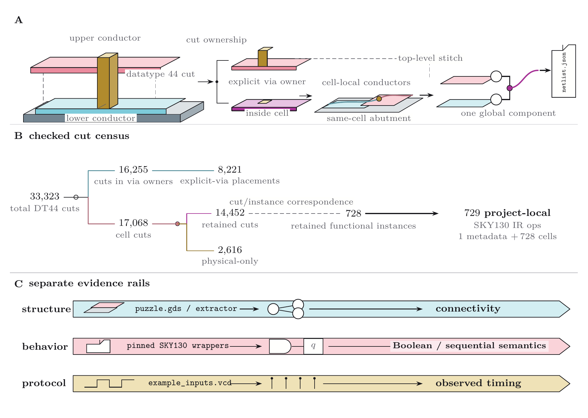
Figure 2. Geometry extraction from GDS polygons to checked logical nets.
But How Do You Know the Netlist Is Right?
Structural Invariants
We need to verify the structures properly before any emulation , so we need to make sure that thr structure was coherant and valid.
The 728 functional cells use 739 distinct component IDs. Cell outputs drive 734
of them, each exactly once. Four more are the primary inputs I, clk,
enable, and rst_n.
That leaves component 61217 which reaches the A1 pins of two gates but has no
recovered cell output, primary input, constant, or the worst one which is no power source.I didnt know what to do with this so rather than
hide it, work/netlist.json you can see it named as
undriven_61217. (DW it will come back later )
Onwards to the vertical connections which offered another POV on our plight . Expanding every placement produced 33,323 datatype-44 cut occurrences. Of these, 16,255 sit inside 8,221 explicit via placements. The other 17,068 occur inside SKY130 cells and pass through the extractor's geometric landing check. Now all 14,452 cuts in retained functional cells overlap selected conductors on both sides. The remaining 2,616 belong to physical-only cells filtered from the logical netlist which includes the 20 one-sided diode cases.
The Warm-Up as an Oracle ?
Jane Street gladly supplied a smaller practice chip with something the puzzle did not
have: source code. It shifts in two eight-bit numbers and raises S when their
sum is 496. so a good function test .
For solving this an exhaustive runner tried every ordered pair of eight-bit
values. Under its fixed harness, all 65,536 pairs agreed with A + B == 496.
Exactly 15 pairs raised S, as the equation predicts.
The work/verification/verify_warmup.py starts from that checked netlist JSON, builds
the source and lowered transition models, then tests 1,034 distinct operand
pairs so all 15 satisfying pairs plus seeded random cases.Read the code for more info.
The exhaustive sweep supports the geometry rules on a known design which we see later in the blog , this helped me form some intuision on how to go on about things later on ...
A Rule for the Rest of the Project
One rule now was to for every representation boundary, give a mistake another way to become visible because we dont have a verifier so this became my priority
Geometry needed structural counts and a known warm-up design. Recovered cell behavior needed the official Verilog models. The serial-input harness needed the supplied waveform. I thought of compiler lowering but would need separate source and target evaluators, a Z3 miter, and mutations designed to make the checks fail.
"separate" here means that two evaluators can take different execution paths while still sharing a parser, verifier, model manifest, or test harness. And those shared parts leave room for common mistakes for me
How Bout We Give the Gates Meaning ?
Why the PDK Headers Were Not Enough
The netlist told me that one instance was an and2_2 and another was an
a21bo_2. The suffix
describes drive strength, but the base name identifies a logical function from
the SKY130 standard-cell library. To execute the chip, I needed a model for
every base cell used by the recovered design which is open source so lets hunt there now .
Vendor the relevant functional Verilog wrappers from the
sky130_fd_sc_hd
library . Across the
combinational wrappers in our solution repo, work/verification/parse_official_models.py extracts scalar ports and
positional gate instances such as and, nor, and buf, then orders them by
their wire dependencies. The resulting ordinary-cell graphs come from the
structure of the official wrappers.
The parser is not a general Verilog frontend tho so it does not handle
arbitrary modules, assignments, vectors, timing, or power behavior and we dont need to care about it now to solve this challenge. It
recognizes the mux wrapper's UDP call tho . The tie
cell uses pull-up and pull-down primitives, and the three supported flip-flop
families need state.
work/extraction/build_cell_manifest.py serializes these definitions into
models/cells.json. The project contains 64 base models, and hashes each functional wrapper.
I used Icarus to run the vendored official wrappers and UDP definitions. The test suite compares all binary inputs for the 60 combinational types and the tie cell, then uses directed tests for mux and flip-flop behavior.
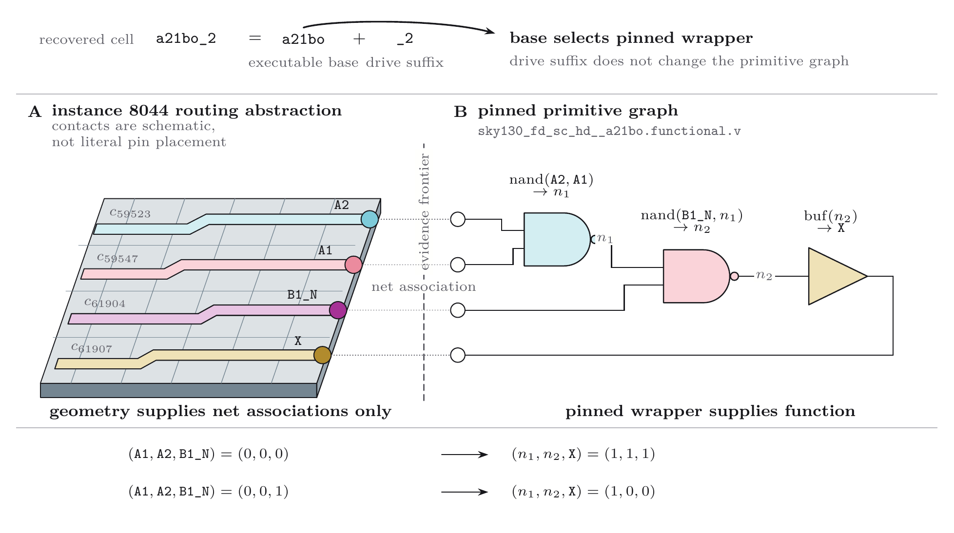
Figure 3. Recovered cell names become pinned SKY130 behavior.
Time Enters the Model
FOr Combinational gates their outputs follow from their current
inputs. Flip-flops make the circuit different. Their output Q is part of the
current state, while their input D determines state after a clock edge. A
useful model therefore has to say not only what each wire means, but also when
values are observed.
Here we can choose a sampled-edge model. One evaluation observes the primary outputs from the current inputs and current flip-flop state, then computes every flip-flop's next value at one abstract positive edge. Also, the Little Ball of Fur edge-sampling docs are a goated resource for graph sampling. In compact form:
outputs(t) = F(inputs(t), state(t))
state(t + 1) = T(inputs(t), state(t))
Onto some explanation . dfxtp simply
captures D. For dfrtp, RESET_B=0 forces the next Q to zero. For dfstp,
SET_B=0 forces it to one. Also while testing the last case help me catch a bug in the legacy
simulator because it compared the control pin with the value to be forced. .
So wrapping it up the current state is an explicit input to this transition function. We dont need the compiler to invent a power-on value(althought ill try this out later after learning more electronics ). Puzzle-specific tools make a separate harness design choice which i can think of writing this would be that : flip-flops with an asynchronous value begin at that value, and the remaining flip-flops begin at zero. And to keep initialization outside the cell semantics.
This model is very much narrower than an event-driven Verilog simulator bc it represents
an asynchronous control as an override when that control is stable at the
sampled edge. We dont need to model immediate changes between edges, propagation
delay, metastability, arbitrary clock waveforms, power, or general X and Z
resolution blah blah .
Reading the Failed Attempts
The supplied VCD's defenition of the input protocol. Which contains two reset-separated trials. In each one,
rst_n stays low for three rising edges. The trace then gives the circuit one
idle edge after reset and raises enable for exactly 121 rising edges. The
serial input I changes on falling edges, so each bit is stable before the
next sample.
At the first rising-edge timestamp after enable falls, O[7:0] begins to
change once per clock:
54 52 59 20 41 47 41 49 4e 00
 T  R  Y     A  G  A  I  N
Uhm the same sequence appears after both input streams
We can use this waveform as evidence for the reset schedule, serial length, and observable failed output. I think that a direct comparison would need to state that phase alignment and handle the trace's initial unknown values.
With connectivity and sampled cell behavior in place, we can move onto figure out which 121-bit stream could take it to an accepting state. >U< actual reversing time ehe
Turning Time Into Logic
Unrolling the Circuit
A simulator answers a forward question: given an input stream, what does the
chip do? I needed the reverse direction: which input stream makes success
true? The transition model made that a bounded symbolic-execution problem.
If you want more background on symbolic execution, I have written about it in another reverse-engineering post:
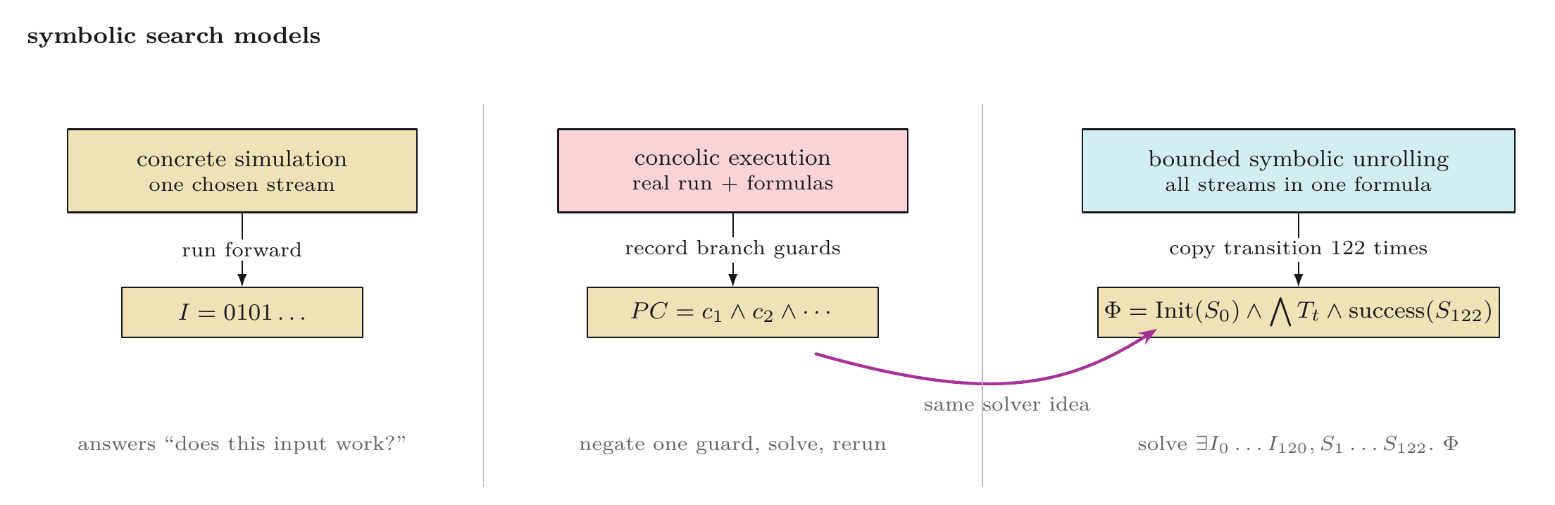
If the reversing and radare UI9yes it looks very messy at times) is not your taste, here's my explanation Concrete execution uses a real input first. Symbolic execution uses a placeholder first.
So instead of trying:
x = 13
we say:
x = some unknown 8-bit value
If the program later computes y = (x xor 0x5a) + 3, then y is a little expression:
y = (unknown xor 0x5a) + 3
So in Symbolic execution it builds a formula and asks the solver to fill in the unknowns that make the target true.
Branches add a path condition." If a program checks if x > 10, then the two paths carry:
then path: x > 10
else path: x <= 10
Concolic execution is the practical hybrid version. It runs once with a real input, records the symbolic path condition, flips one branch condition, asks a solver for a new input, and runs again.
For this ASIC puzzle, after lifting it i had a clocked circuit. Each clock edge takes the current flip-flop state plus one input bit and produces the next flip-flop state:
next_state = T(current_state, input_bit)
The unknown key is 121 bits:
K = k_0, k_1, ..., k_120
Unrolling means copying the same transition step across time:
S_1   = T(S_0,   k_0)
S_2   = T(S_1,   k_1)
...
S_121 = T(S_120, k_120)
S_122 = T(S_121, 0)
Then Z3 gets one big question:
Find k_0..k_120 such that every clock step is valid
and success is true after the verdict edge.
This is much better than brute force. Symbolic unrolling still creates a large formula, but the formula follows the circuit structure .(This is an into if youre interested to get into taint analysis)
These were also useful while I was learning symbolic execution. My first practical intro to angr was this beginner reverse-engineering walkthrough from john hammond , so I recommend starting there before jumping into the papers:
- INGoogle CTF, Beginner Reverse Engineering with ANGR, by John Hammond.
- angr. A practical symbolic-execution framework for binary analysis and reverse engineering.
- James C. King, Symbolic Execution and Program Testing. The first paper from 1976 for executing over symbols instead of concrete inputs: https://research.ibm.com/publications/symbolic-execution-and-program-testing
- Cristian Cadar, Introduction to Dynamic Symbolic Execution and KLEE. A longer academic tutorial if you want something more rigorous: https://wp.cs.ucl.ac.uk/tarot2018/talks/
- DART and CUTE. The classic 2005 concolic or dynamic symbolic execution papers: https://osl.cs.illinois.edu/publications/conf/pldi/GodefroidKS05.html and https://osl.cs.illinois.edu/publications/conf/sigsoft/SenMA05.html
- KLEE. A practical symbolic-execution system for generating high-coverage tests and finding real bugs in systems programs: https://llvm.org/pubs/2008-12-OSDI-KLEE.html
Now let S_t be to denote all 92 flip-flop values before edge t, and let I_t be the
serial input on that edge. One step of the recovered circuit defines
S_(t + 1) = T(S_t, I_t)
Lets create fresh
Z3 Boolean variables k_0 through k_120. k_0 is simply the first bit
sampled in time; no integer endianness or grid interpretation is needed yet(very fun stuff if you wanna dig into why it would not be needed here ), then we can
copy the transition relation across the input window, feeding each
state expression into the next edge.
And now our harness should fix everything that is not part of the key. Flip-flops with an
asynchronous value start at that value, while the others start at zero.
rst_n remains high, undriven_61217 is fixed to zero, and enable stays high
for all 121 symbolic bits.
After the last bit, I set I=0, lowered enable, and took one more transition.
That is like the verdict edge. Because the model exposes outputs before each abstract
edge, I asked for success=1 in the following frame. And now we have
121 enabled transitions and one disabled transition
So our current checker treats only the first 121 as symbolic key material and rejects a fixture whose tail is not all zero.
Finally after messing around a lot , we get the accepting output and we can use Z3 for a model. The solver returned a concrete 121-bit stream.
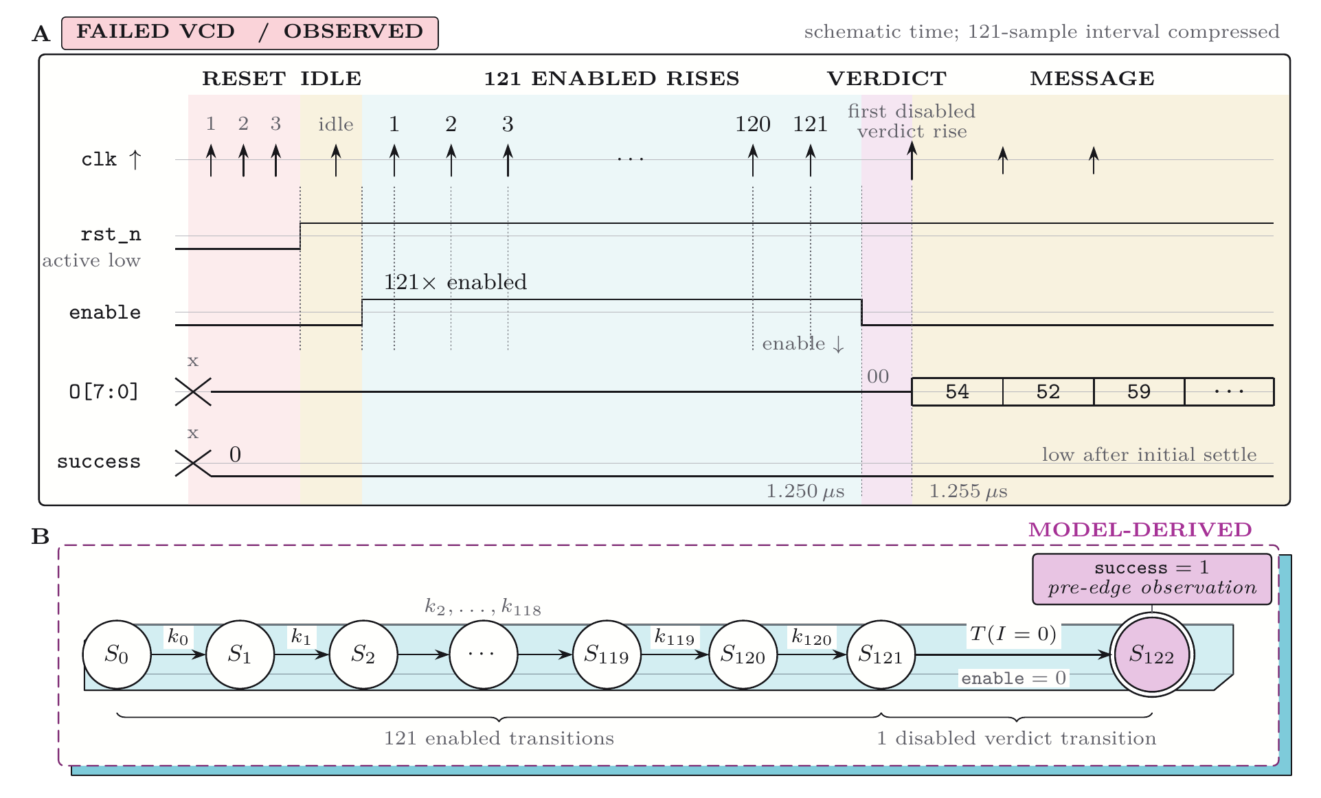
Figure 4. Protocol timing and 121-step symbolic unrolling.
Is There Another Key tho ?
An important thing to keep in mind is that one satisfying input does not imply a unique input. To check that,
work/verification/verify_key_uniqueness.py has the acceptance formula from the serialized
recovered-cell model and solves it without constraining the key to the retained
answer.For the first query it returns SAT.
Lets add one more blocking clause:
(k_0 differs) OR (k_1 differs) OR ... OR (k_120 differs)
The acceptance constraint remains in place. The second query asks ie means that whether any different 121-bit stream can succeed under the same harness. Z3 returns UNSAT.
This is a bounded uniqueness statement,which holds true for the current binary
SKY130 source model, the fixed initial state, rst_n=1,
undriven_61217=0, 121 enabled samples, I=0 afterward, and one disabled
verdict edge.
Asking a Different Simulator mhmm
The symbolic solve still depended on my Python interpretation of the cells. To
test that interpretation through a different execution engine,
work/verification/verify_gate_simulation.py emits a temporary gate-level Verilog module directly from
the checked netlist.
The Stars Appear drum rolls please
The protocol had contained 121 samples, so I tried laying Z3's result out as an
11-by-11 grid. Under a row-major interpretation, I placed the first
sample in the upper-left corner, continued from left to right, and wrapped
after every eleven bits. Replacing zero with . and one with * produced:
.......*.*.
*....*.....
.......*.*.
*.*........
....*.*....
..*.....*..
....*.....*
.*....*....
...*......*
.....*..*..
.*.*.......
YEY so as you can see stream contains 22 one-bits. Every row has two. Every column has two. I also checked every horizontal, vertical, and diagonal neighboring pair; no two ones touch. The grid met the row, column, and no-touch rules of a two-star Star Battle.(the region boundaries are missing but who cares lol )
Star Battle also requires irregular regions, with exactly two stars in each region.
Lets try replaying the stream through the source and lowered interpreters named the
puzzle explicitly. After the 121 enabled samples, the circuit took one
disabled verdict edge. In the following pre-edge frame, success was high and
the output bus began emitting:
(* TWO STARS *)
The printable message contains 15 bytes, followed by a zero byte which is our answer .
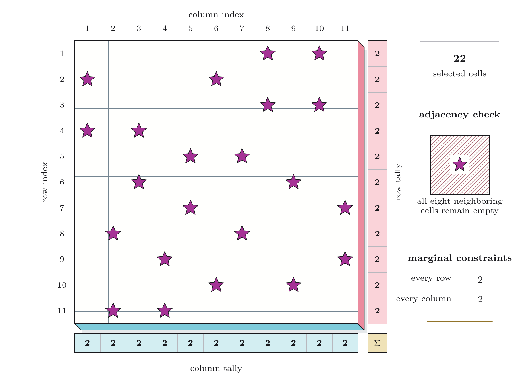
Figure 5. The accepted 121-bit stream as an 11-by-11 star grid.
Phew , The Regions Were Hiding in State
From One-Hot Inputs and adding Sensitivity Supports >U<
Well if you read until here now theres a good question to ask: were the missing region boundaries also present in the circuit? Rather than identify every counter by hand, I treated the final flip-flop state as a set of probes :)
work/verification/recover_regions.py begins with the current lowered model, translation-
validated under IND-1, and the same explicit initial-state rule used by the
puzzle harness. It first runs
an all-zero serial stream. Then it runs 121 more streams, each from a fresh copy
of the initial state. Stream c contains a single one at input position c
and zeros everywhere else.Every stream has 121 enabled transitions followed
by 20 disabled tail transitions, with rst_n=1 and undriven_61217=0.
For each of the 92 state bits, I compared its final value in every one-hot run with its final value in the all-zero baseline. Okie let this define a support:
support(q) = { c | final_q(one_at_c) differs from final_q(all_zero) }
Also if a state bit was part of a counter associated with some set of grid cells, its support could reveal that set. The current probe found 43 state bits with nonempty supports. Eight supports were disconnected on the 11-by-11 grid. The remaining 35 distinct supports are connected using only up, down, left, and right neighbors.
All-zero baseline refers to the input stream btw and four active-low-set flip-flops begin at one, and the final baseline state contains eleven ones. The probe also observes only the state after its fixed 20-cycle tail. So Why track any intermediate change ??
Two Covers
Next I treated the 35 connected supports as candidates and searched for exact covers: choose e eleven supports that are pairwise disjoint and cover all 121 cells. The search found two answers mhmm ?
The first answer was the eleven literal columns. Each support contained one column from top to bottom. The second answer was this irregular partition.
AAAAABBCDDE
AAFAABCCDDE
AAFBBBBCCDE
AAFBGGGECCE
FAFBGEEEEEE
FFFBGGGEHHH
BBBBBBGEHII
BJJJGGGEHII
BJJKEEEEHII
BBJKKEEEHHH
BJJKEEEEEEE
The letters are presentation labels assigned after the cover is chosen Selecting the irregular cover as the puzzle regions requires assumptions.Lets record them
- The 121 enabled samples map row-major to an 11-by-11 grid.
- Intended regions are connected through four-neighbor adjacency.
- The region partition appears as eleven disjoint supports under this final-state probe.
- The region-counter bank is distinct from the literal-column counter bank.
Now under those assumptions, the irregular partition is the sole non-column connected cover produced by the observed supports.
I probed the model, built the
supports, found both covers, identified the literal columns, and selected the
sole non-column cover before loading work/solution_bits.txt. Only afterward
did I annotate the selected regions with stars and check that each one contains
two. The final regions.json therefore contains key-derived validation fields,
but the choice between covers is keyless lol
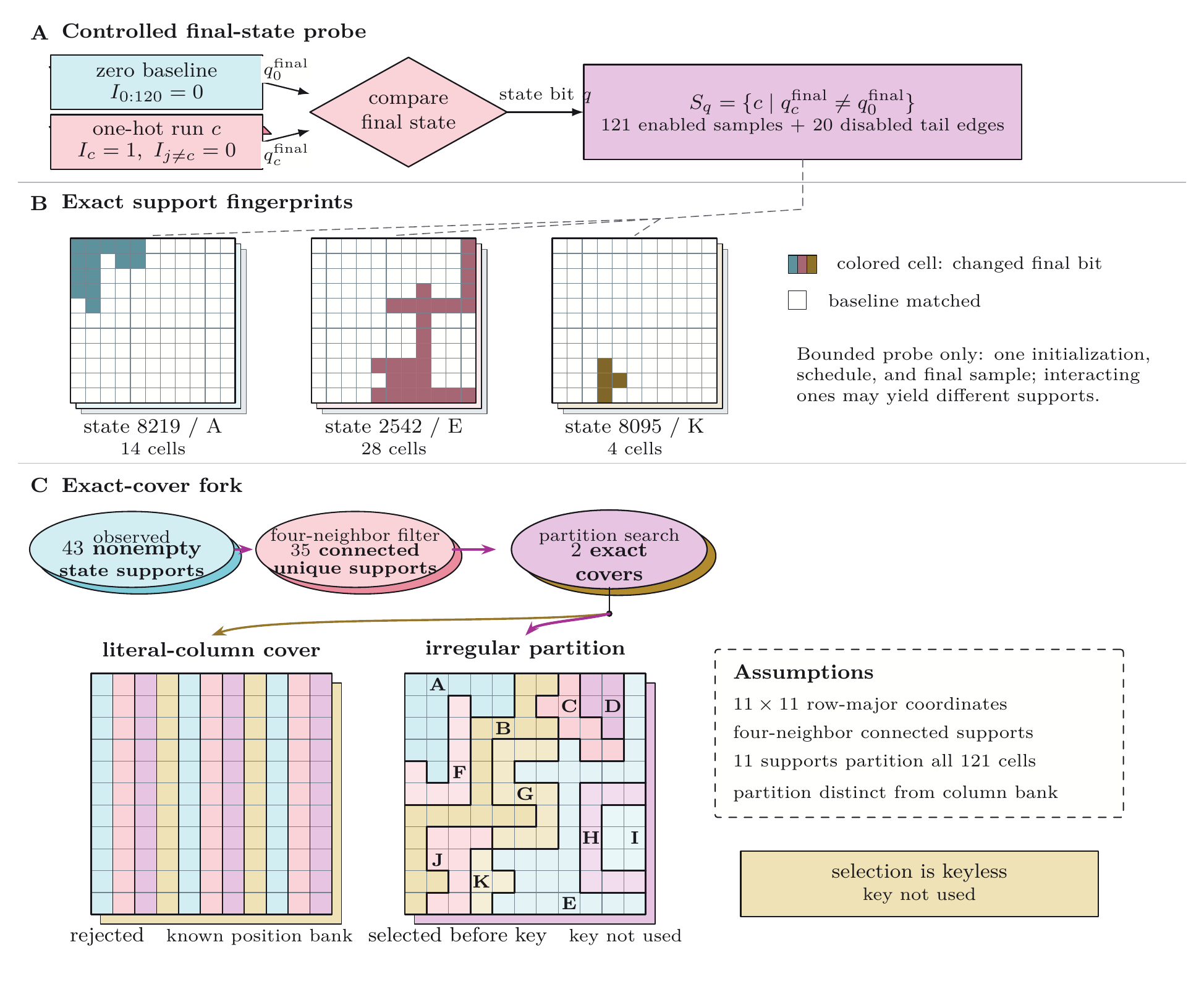
Figure 6. One-hot supports reduce to two exact region covers.
Solving the Recovered Regions Without the Key
Well I wrote a standalone Star Battle solver that uses only the irregular region grid.
Its depth-first search places two stars in each row. It rejects a placement as soon as a column or region would exceed two stars, or a new star would touch an existing one horizontally, vertically, or diagonally. The search stops after finding two solutions. If it returns one, it has exhausted every remaining branch and established uniqueness; if it returns two, the puzzle has at least two.
For the recovered grid, the search found one solution.
The verification scripts regenerate the region artifact from the current
lowered transition model and require byte-for-byte equality with
work/regions.json if yall wanna see .
So What is this Circuit even about ?
Is this a Checker ?
So the circuit checks the bits as they arrive instead of storing it someplace and checking it .
Two four-bit position machines track the current column and row. They only progress if the
effective sample is accepted, so lowering enable pauses the
board r. A twelve-bit shift window retains the most
recent accepted inputs for adjacency checks. At the same time, small counters
accumulate stars by row, column, irregular region, and total population.
Sticky flags remember whether any completed row was bad or any touching pair
was seen.
The 92 flip-flops can be categorised based on what we found .
| Role | Flip-flops |
|---|---|
| Previous input bits | 12 |
| Row and column position | 8 |
| Eleven column counters | 22 |
| Eleven irregular-region counters | 22 |
| Current-row count and row-error flag | 3 |
| Touch-error flag | 1 |
| Total-star count | 8 |
| Completion and verdict control | 4 |
| Message address | 4 |
| Rolling output-generator state | 8 |
Only the history register stores literal past inputs, and it keeps only the latest twelve. At completion those states contain cells 109 through 120. The rest of the machine stores position, capped counts, rolling summaries, and sticky facts. It remembers like about the stream to decide the puzzle(should have stored it in someplace and we could have cheesed it even more with just normal symoblic execution )
The effective sampling condition is enable AND NOT complete. On the final
cell, every counter and error latch still sees the current bit, and the same
edge raises completion. From then on the effective condition stays false even
if external enable remains high and the next edge evaluates the accumulated
state and starts the output phase.
Checking Neighbors With Twelve Bits of History
In row-major order, a current cell can touch four cells that have already arrived:
| Offset | Grid position |
|---|---|
t - 1 | left |
t - 10 | up-right |
t - 11 | up |
t - 12 | up-left |
The twelve history flip-flops form an enable-controlled shift register. Before
the edge accepting sample t, its first stage contains t - 1 and its last
stage contains t - 12. The current input remains a combinational value beside
that window. Disabled edges hold every stage
so these are accepted-sample offsets .
Three taps need column-boundary guards. In the first column, t - 1 would be
the previous row's final cell and t - 12 would also wrap incorrectly. In the
last column, t - 10 points at the current row's first cell rather than an
up-right neighbor. The column-position state suppresses those cases. The
t - 11 tap never wraps and good for us .
If the current bit and any valid prior-neighbor tap are both one, the circuit sets a sticky touch-error flag. Checking only four directions is enough for this then the other four directions belong to future cells, and each pair is detected when its later endpoint arrives. Across an 11-by-11 grid, the taps cover all 110 horizontal, 110 vertical, and 200 diagonal neighbor pairs and we also need Every real unordered touching pair is checked once cuz ofc .
How about we Count Without Remembering the Grid
Rows, columns, and regions need counts. The circuit uses a two-bit saturating code:
zero       00
one        10
exactly two 01
three or more 11
On each hit the sequence is 00 -> 10 -> 01 -> 11, with 11 absorbing. So we can actually
distinguish the only four cases the checker needs .
At column ten, the circuit includes the current bit, checks whether the completed row total is exactly two, records any failure in a sticky row-error latch, and resets the two counter bits for the next row. The circuit therefore should and must reuses three state bits across all eleven rows: two for the count and one for accumulated failure.
Also columns cannot be reused because all eleven remain active while the board streams past. They receive eleven persistent two-bit counters, selected by the column-position decoder. The irregular regions receive another eleven two-bit counters, selected by row-and-column membership logic. One input star therefore increments exactly one row count, one column count, one irregular count, and the total population count in parallel.
The total counter is an ordinary eight-bit binary incrementer and cannot wrap during a 121-cell run. The terminal cone contains a separate decoder for the unique eight-bit encoding of 22. That check's logic is if every one of eleven columns contains exactly two stars, the total must already be 22.
At the end the row latch we can identify that the two sticky error bits and the persistent counters compress the whole stream into terminal facts and with the row latch says whether every row was valid. The touch latch says whether any forbidden pair appeared. The column and irregular banks retain capped counts, while the total counter retains the population
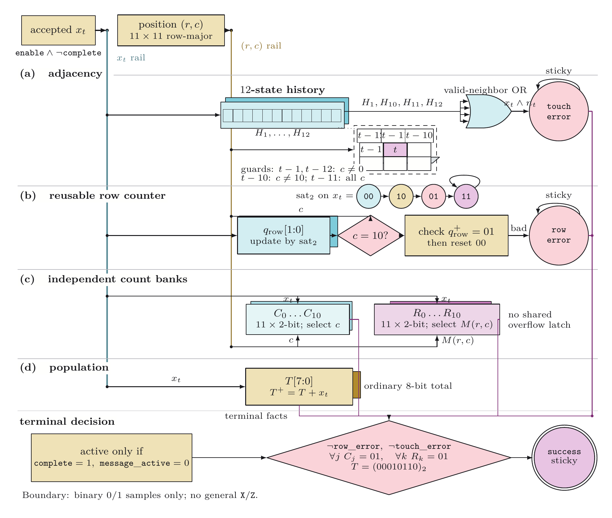
Figure 7. Streaming checker state for rows, regions, population, and adjacency.
The One-Cycle Verdict Window
The following frame has a phase that occurs once in normal operation:
complete = 1
message_active = 0
The result latch samples the accumulated terminal condition.
That condition requires the completion phase, eleven exact-two column counts,
eleven exact-two irregular counts,and the
intended total-count state. The same edge raises message_active, whether the
input was accepted or rejected.
Completion is sticky, and so is message-active
follows completion . Once message-active becomes one, the
phase complete=1, message_active=0 cannot recur until reset.
On a normal accepted run, success rises on that verdict edge and stays high
until reset. Arbitrary injected states need not behave the same way if they come up in your test case ..
A Sequencer to get the answer
Message output uses two separate pieces of state and Four flip-flops form an address sequencer. while message-active is low their next-state logic drives them to zero, so they settle before we get anything . A separate bank of eight flip-flops evolves with the input stream and contributes to the generated bytes.
To avoid inventing numeric significance for the four physical address bits,
lets write them in state-ID order (234, 235, 236, 237). During message mode they
follow:
0000 -> 0100 -> 0010 -> 0110
     -> 1000 -> 1100 -> 1010 -> 1110
     -> 0001 -> 0101 -> 0011 -> 0111
     -> 1001 -> 1101 -> 1011 -> 1111
The sequencer visits all sixteen patterns once, then remains at 1111.
The address, rolling generator state, population count, and verdict mode feed the combinational byte decoder. For an accepted input, the fifteen transient addresses produce :)
(* TWO STARS *)
and 1111 forces O[7:0] to NUL forever. Rejected inputs use the same address
path but different byte-selection logic; the ordinary failure mode produces
TRY AGAIN.
One thing i remember is from an year ago i remember authoring a reverse engg challenge which was a custom chip 8 implementation so this is kinda unusual than a ROM indexed by a counter. The chip carries a rolling eight-bit summary during input, latches a verdict mode, walks a nonnumeric four-bit address path, and combines those pieces for our reply
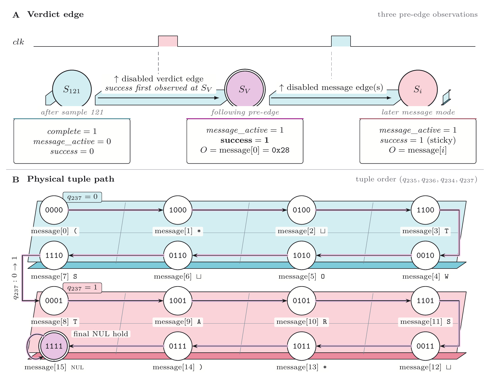
Figure 8. Verdict timing and message-byte address order.
Can i make a decompiler ????
By this point, the project had an extractor, simulator, symbolic solver, region probe, and several checkers. I had a model manifest kinda stuff which removed some duplication, but it did not create a clean boundary. Port ordering, state ordering, output mapping, clock policy, and undriven-net handling still appeared in several places. The thing is many wrong transition models can agree on one successful path.
An intermediate representation [ will be abbreviated to IR] , the first textual-IR slice did not solve this fully , i made it emit both a SKY130 layer and a lower-level Silicon layer, but generated each one independently from the same netlist. The target looked like the result of a lowering pass but didnt actually use the source artifact. In my current path , it validates the checked netlist, emits one source operation per recovered cell, serializes and reparses the source, then gives only that reparsed source module and the model manifest to the lowerer. The target is serialized, reparsed, and verified in turn as well. Simulation, symbolic validation, and puzzle analysis can then use the results those explicit representations instead of rebuilding cell semantics ad hoc.
The hard part is controlling semantic change , the hard part is as you guessed recovered physical-cell vocabulary on one side, a small Boolean transition vocabulary on the other, and checks around the transformation between them , for this I have defined a narrow profile called IND-1 .
A Tiny IR for Recovered Silicon
Why Build a Custom IR?
(it's a really small IR ) My inspiration was from MLIR from learning LLVM . MLIR stuff like modules, SSA names, typed function signatures, quoted operation names, and attribute dictionaries. The implementation is in Python.
The source layer has sky130.cell operation for every recovered instance.
Each operation records its instance ID, base model, original
drive-strength-qualified cell name, ordered pins, operands, and results. Module
metadata binds the representation to the netlist and model-manifest hashes and
records the clock, state order, output order, and pre-edge observation rule(this can be improvised and i will come back to it in the future).
Flip-flop state is in the @step function which takes
92 current-state bits as arguments and returns 92 next-state bits before its
nine primary outputs.A
simulator can carry returned state into another call; a solver can replace the
arguments with symbolic values; a miter can compare two implementations of the
same function.
The target layer uses only constants, Boolean gates, muxes, and explicit DFF next-state operations. This canonical form is less descriptive of the physical library but easier for analyses(passes like stuff in the future ) to execute.
The IND-1 Boundary
IND-1 describes one binary sampled transition. Its validated boundary starts at
the checked work/netlist.json. It would have taken me a lot more time to do from GDS so extract the netlist for this .
A valid input uses only the 64 pinned SKY130 base models in the manifest. Nets are scalar, consumed nets have one driver, and the combinational graph must be acyclic. The design may have one declared positive-edge input clock, reached directly or through supported clock-buffer chains.
One call returns pre-edge primary outputs and post-edge state and each client must choose or quantify over current state. That is why the translation miter can cover arbitrary binary states if you got it.
One Legitimate Lowering Path
At the end after a lot of failing and thinking , this was the compiler lowering pass design stucture i designed
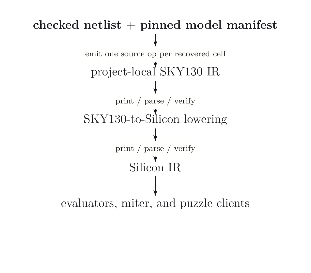
The source artifact contains 729 operations: one metadata operation and 728 cell operations. Combinational cells remain at library level, constants keep their source pins, and every flip-flop operation consumes its explicit current state and produces one next-state result.
The lowerer accepts a source module and the manifest. It accepts no netlist
object, so source operands and SSA results provide connectivity. Combinational
model DAGs expand into binary not, and, or, xor, and mux operations.
Buffers become SSA aliases. Tie-cell outputs become constants. Each source
flip-flop becomes one silicon.dff operation with explicit data, clock,
current-state, and optional sampled asynchronous-control operands.
The puzzle target contains 1,541 operations, including metadata, twelve constants, and 92 DFF transitions.
The source is printed, parsed into a fresh AST, and verified before lowering. The target is verified, printed, parsed again, and verified again. Only after both layers pass are the output files replaced : )
Checking the Lowering with Z3
Separate Executions of Source and Target
The source
evaluator walks sky130.cell operations and interprets each model through the
manifest's primitive graph. The target evaluator handles canonical constants, gates, muxes, and DFF
next-state operations.
Counterexample
The miter creates one Boolean symbol for each represented non-clock input and current-state bit. The puzzle has four such inputs and 92 state bits, for 96 public symbols. The clock is fixed to the active-edge value because one IND-1 call already represents that edge.
One symbolic evaluator expands the serialized SKY130 operations through the values we have set up . Another expands the serialized Silicon operations directly. Each produces 101 values:
92 next-state bits + 9 pre-edge primary outputs
For every paired result, the checker creates a mismatch expression. It ORs all 101 mismatches and asks Z3 whether any assignment to the 96 symbols can make that root true. A SAT result would include a concrete input and current state that distinguish the artifacts. For the current puzzle translation, Z3 returns UNSAT.
The ending result we got was under IND-1 binary sampled-edge semantics and no assignment to the four represented non-clock inputs and 92 current-state bits makes the serialized source.
Oh and about the blocked key unroll and Star Battle enumeration are separate arguments. Their UNSAT and uniqueness results should not be merged with this one.
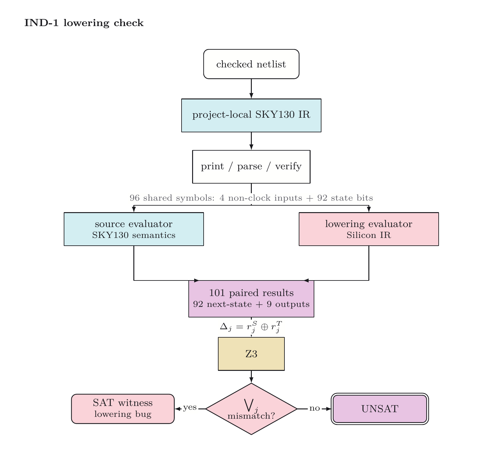
Figure 9. IND-1 lowering checked by a Z3 miter and regression cases.
Returning to Official Models
The miter can only compare the two semantics I wrote. To check those semantics against the library source.
At cell level, Icarus exhaustively checks every binary input combination for 60 combinational types and the tie cell, comparing 848 output bits. Eight directed mux cases exercise four-state behavior, and twenty directed observations cover the three supported flip-flop families. These cases are especially important for the mux UDP and explicit reset/set mappings that the small model parser does not derive in full.
At kinda the whole level the puzzle check uses 128 seeded arbitrary-state one-step assignments. Each compares nine pre-edge outputs and 92 post-edge state bits, for 12,928 bit comparisons. A smaller warm-up run contributes 272 more. As as i said earlier, these are independent assignments rather than state-carrying protocol streams
Icarus provides a separate execution engine and runs the official wrappers and UDPs inside the emitted device , think of this as an external oracle .
This file here work/ind1_evidence.json records the model and artifact hashes, library commit,
tool versions, seeds, miter formula hash, mutation results, and semantic-loss
ledger.
Why Use a Compiler Without Optimization?
I mean there is no optimizer in this pipeline, and we dont also need it and it would be useless ofc . Canonicalization turns a library-specific netlist into a stable transition language. Parsing, verification, and translation validation make each semantic change inspectable. In reverse my opinion is that, knowing exactly which changes occur matters more.
What I Learned from the Chip
The hardest part of this puzzle was deciding what formula deserved to be solved.
I attached sampled behavior to cell names without trying to model timing or power and made state explicit before unrolling the circuit, and made the lower-level IR consume the source representation .
Once the transition system was almost done , the solver could find an accepted stream and the resulting bits showed the results which was the the star placement. The final state then revealed candidate region structure through sensitivity supports : )
Uniqueness belongs to one recorded harness and region recovery produces two covers and selects the irregular one under stated assumptions. The compiler miter covers one binary transition.
Conclution
At first when i saw this GDS i was dumbfounded but as it went on i applied what my fundementaly about reversing at the end one chain could be followed from a pin shape, through a recovered net and cell, into a state update, a puzzle constraint, and finally a star on an 11-by-11 board
The latex diagrams are based on : https://www.bsaver.io/misc/pretty-figures check it out .
Thankyou to my roomate Nathan and L3AK team for motivating me always yall goated .
The full solution with my lifters and IR model is here: mooofin/jane-street-ASIC-solution .
 Start
Start